Chip giant to provide AI accelerator chips for Japanese firm
Samsung Electronics revealed its plans, Tuesday, for establishing a chip ecosystem with domestic fabless clients during the company’s foundry forums.
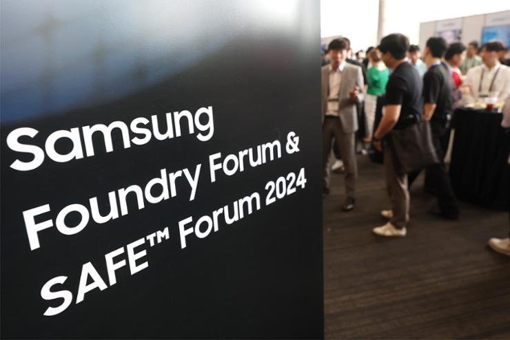
The semiconductor giant held the Samsung Foundry Forum and Samsung Advanced Foundry Ecosystem Forum at COEX in southern Seoul, with 35 partner companies in the fields of semiconductor design, intellectual property, testing and packaging, setting up booths to draw the attention of prospective clients.
“For collaboration with domestic fabless clients, Samsung Electronics is providing various specialty technologies as well as most advanced technologies,” Choi Si-young, head of Samsung Electronics’ foundry business, said during the event.
“Samsung will provide the most essential artificial intelligence solutions to our clients by integrating specialty solutions, including BCD.”
Samsung describes a string of technologies required for functions such as embedded memory, image sensors and radio frequency as the specialty process. BCD — short for bipolar, CMOS and DMOS — is a set of silicon processes, each of which combines the strengths of three different process technologies onto a single chip.
During the forum, Samsung proposed its foundry business strategy that can provide integrated turnkey AI services tailored to various clients’ needs, leveraging its strengths as a chipmaker covering foundry, memory chips and packaging.
Specifically, the company stressed that it plans to strengthen foundry services using advanced technologies such as gate-all-around (GAA) transistor architecture and 2.5-dimension packaging technology.
Read More
- Samsung vows to offer one-stop AI chip foundry solution to match TSMC
In line with this, the company announced it will provide turnkey semiconductor solutions using the 2-nanometer (nm) foundry process and 2.5D packaging technology called I-Cube S to Preferred Networks, a leading Japanese AI company, in collaboration with Korean system semiconductor developer Gaonchips.
I-Cube S is a technology for packaging multiple chips together to enhance interconnection speed and reduce package size.
“This order is pivotal as it validates Samsung’s 2-nm GAA process technology and advanced packaging technology as an ideal solution for next-generation AI accelerators,” said Song Tae-joong, vice president of the foundry business development team at Samsung Electronics.
“We are committed to closely collaborating with our customers, ensuring that the high performance and low power characteristics of our products are fully realized.”
By leveraging Samsung’s leading-edge foundry and advanced packaging products, Preferred Networks aims to develop powerful AI accelerators that meet the ever-growing demand for computing power driven by generative AI, Samsung said.
During the event, the company promised to provide proactive services to its domestic design solutions partners to help fabless firms expand their presence in the AI market.
Last month, the company held the Samsung Foundry Forum and Samsung Advanced Foundry Ecosystem Forum in San Jose, California, unveiling its vision and technology roadmap for the AI era. Samsung Electronics plans to hold the forums in Japan and Europe in the second half of this year.


